


Technical Information Note
Target material selection for coating SEM samples
using an SEM sputter coater
Introduction
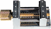
The coating material for making a non-conductive SEM sample conductive should be selected to achieve optimum performance. There is no such thing as a universal coating materials and target materials might vary for different sample materials and desired results. Most SEM sputter coaters allow for an easy and quick target chance, thus selecting and using the optimum target material doesn't require a lot of effort.
When using other coating (target) materials than Gold, the use of lab grade Argon as process gas is paramount. The coating quality is affected by the target material, process parameters and by the interaction with the sample material. Benefits of coating non-conductive SEM samples are:
- Coating an SEM sample with a highly conductive metal makes non-conductive SEM samples conductive to avoid charging of the sample surface. Enabling higher resolution imaging due to higher sample stability under the electron beam
- Most coating materials have a (much) higher secondary electron (SE) yield than the non- conductive sample materials. In most cases, coating SEM samples with only a nm of Au or Pt increases the signal to noise ratio dramatically, resulting in crisp and clear images
Below some practical guidance information for selecting the target material and expected grain size of the coating is given. The information is only valid when using a modern DC magnetron SEM sputter coater with Argon as process gas. Grain size of the coating depends strongly on coating thickness and coating material/sample material interaction. Using standard coating conditions and coating similar sample materials the following grain sizes can be expected:
Gold, silver: 5-10nm
Palladium: 5-10nm
Gold/Palladium: 4-8nm
Platinum: 2-3nm
Iridium: 1-2nm
Chromium: 1-2nm
Tungsten: <1nm
If EDX analysis of the sample is needed, try to select a coating (target) material which is not present in the sample. This would avoid overlapping peaks in the EDX spectrum or confusion within the EDX analysis.
Selection guide table for target materials for SEM, FESEM and EDX applications
|
Target Materials |
|||||||||||||
Application |
Au |
Au/Pd |
Ag |
Pt |
Pt/Pd |
Ir |
Cr |
W |
Ta |
Pd |
Ni |
Cu |
Ti |
C* |
Low and medium magnifications |
V |
V |
V |
V |
V |
V |
- |
- |
- |
V |
V |
V |
- |
V |
High resolution imaging |
- |
- |
- |
V |
V |
V |
V |
V |
V |
- |
- |
- |
- |
V |
Ultra-high resolution imaging |
- |
- |
- |
- |
V |
V |
V |
V |
V |
- |
- |
- |
- |
V |
SE signal boost (1nm or less) |
V |
- |
- |
V |
- |
V |
- |
- |
- |
- |
- |
- |
- |
- |
BSE imaging |
- |
- |
- |
- |
- |
- |
V |
- |
- |
V |
- |
- |
- |
V |
Table top SEM coating with air |
V |
- |
- |
- |
- |
- |
- |
- |
- |
- |
- |
- |
- |
- |
Gold colloids imaging |
- |
- |
- |
- |
- |
- |
V |
- |
- |
- |
- |
- |
- |
V |
EDX analysis |
- |
- |
- |
- |
- |
- |
V |
- |
- |
- |
V |
V |
V |
V |
Light element analysis |
- |
- |
- |
- |
- |
V |
- |
- |
- |
- |
- |
- |
- |
- |
EBSD (2-3nm) |
V |
- |
- |
V |
- |
V |
- |
V |
- |
- |
- |
- |
- |
V |
* Carbon evaporated in a high vacuum coater
- Coating material with lower atomic numbers is more suitable for BSE (back scattered electron) imaging.
- Coating with higher atomic numbers is more suitable for SE imaging.
Physical properties of target materials for small desktop sputter coaters.
Target Metal |
Symbol |
Atomic Number |
Atomic weight |
Density g/cm3 |
Melting point °C |
Carbon |
C |
6 |
12.011 |
2.27 |
3500 |
Magnesium |
Mg |
12 |
24.305 |
1.74 |
650 |
Aluminium |
Al |
13 |
26.982 |
2.70 |
660 |
Titanium |
Ti |
22 |
47.88 |
4.51 |
1668 |
Vanadium |
V |
23 |
50.942 |
6.11 |
1910 |
Chromium |
Cr |
24 |
51.996 |
7.14 |
1907 |
Manganese |
Mn |
25 |
54.938 |
7.47 |
1246 |
Iron |
Fe |
26 |
55.847 |
7.87 |
1538 |
Cobalt |
Co |
27 |
58.933 |
8.90 |
1495 |
Nickel |
Ni |
28 |
58.7 |
8.91 |
1455 |
Copper |
Cu |
29 |
63.546 |
8.92 |
1085 |
Zinc |
Zn |
30 |
65.39 |
7.14 |
420 |
Zirconium |
Zr |
40 |
91.22 |
6.51 |
1855 |
Niobium |
Nb |
41 |
92.906 |
8.57 |
2477 |
Molybdenum |
Mo |
42 |
95.94 |
10.28 |
26.23 |
Palladium |
Pd |
46 |
106.42 |
12.02 |
1555 |
Silver |
Ag |
47 |
107.868 |
10.49 |
962 |
Indium |
In |
49 |
114.82 |
7.31 |
157 |
Tin |
Sn |
50 |
118.71 |
7.31 |
232 |
Tantalum |
Ta |
73 |
180.948 |
16.65 |
3017 |
Tungsten |
W |
74 |
183.85 |
19.25 |
3422 |
Iridium |
Ir |
77 |
192.22 |
22.65 |
2466 |
Platinum |
Pt |
78 |
195.08 |
21.09 |
1768 |
Gold |
Au |
79 |
196.967 |
19.3 |
1064 |
Lead |
Pb |
82 |
207.2 |
11.34 |
328 |
Target Alloy |
Composition wt% |
Weighed Atomic Number |
Weighed Atomic weight |
Density g.cm3 |
Melting point °C |
Gold/Palladium |
Au/Pd 80/20 |
72.4 |
178.858 |
17.84 |
1440 |
Gold/Palladium |
Au/Pd 60/40 |
65.8 |
160.748 |
13.98 |
1350 |
Platinum/Palladium |
Pt/Pd 80/20 |
71.6 |
177.35 |
19.28 |
1760 |
Gold
Gold is the most widely used coating material to coat non-conductive samples for standard SEM applications. Due to its low work function it is a very efficient to coat. When using cool sputter coaters whilst sputtering thin layers, there is hardly any heating of the sample surface. The grain size is visible when using high magnifications on modern SEMs. Gold can be used for low and medium magnification applications and is an ideal coating material for table top SEMs with air as process gas (the gold structure is not imaged due to the reduced resolution of table top SEMs).
A method to remove gold from fossil type SEM sample can be found in this PDF: Removing gold from SEM samples.
Gold/Palladium
The Au/Pd alloy (60/40 and 80/20) is less efficient to coat than with pure gold, which results in lower sputter rates. Au/Pd is often recommended to achieve a smaller grain size. Au/Pd does result in smaller grain sizes when evaporated in high vacuum, but when used in SEM sputter coaters the difference between Au and Au/Pd is hardly visible. Less suitable for heat sensitive specimens and less suitable for EDX analysis due to the extra set of peaks for Pd.
Silver
Ag is a most suitable and lower cost alternative for Au in many imaging applications for low and medium magnifications ranges. It is a widely underestimated coating material. Ag has the highest conductivity of all metals. When using EDS, Ag is an alternative for Au on many biological samples if P, Cl and S need to be analyzed. The sputtering rate is similar to Au, the SE yield is somewhat lower than for Pt, Au or Ir. The grain sizes is similar or slightly larger than Au, except for samples containing halogens which can exhibit coarser grains. The Ag coating can tarnish (in the presence of halogens) and is less suitable for long term storage. Excellent low cost coating material for less demanding imaging applications and table top SEMs.
An additional advantage is that the Ag coating can be dissolved and the sample surface can be studied afterward in original conditions. Removal of Au, Au/Pt, Pt and Ir coatings is more difficult and involves very harsh chemicals. The Ag coating can be removed with Farmer's reducer (Mixture of Potassium Ferricyanide and Sodium Thiosulfate)
Platinum
Pt has a finer grain size than Au or Au/Pd and is therefore more suitable for higher magnifications applications. Excellent SE yield. The higher work function results in a lower sputtering rate than for Au. Pt tends to be sensitive for “stress cracking” when oxygen is present (porous sample can be a source of oxygen). More expensive than Au due to higher fabrication costs.
Platinum/Palladium
Pt/Pd alloy (80/20) has a similar small grain size and SE yield as pure Pt, but it is less sensitive to “stress cracking”. Suitable all-round coating material for FESEM applications when thin coatings are used. Best results are achieved when using high resolution sputter coaters.
Iridium
Ir exhibits a very fine grain size on virtually all materials and is an excellent all-round fine grain coating material for FESEM applications. It is the material of choice for high and ultra-high resolution FESEM imaging. With the added benefit of being a non-oxidising material and a high SE yield, it has been replacing Chromium for high resolution sample coating. It requires the use of a high resolution sputter coater and it has lower sputtering rates. The targets are thicker due to fabricated constraints, but overall costs are lower than for Pt or Pt/Pd. Ir is also an excellent alternative coating material for coating samples which have to be analyzed for carbon by EDX or WDX. A thin layer is enough to create excellent conductivity and since the material is very rare it hardly interferes with EDX or WDX analysis.
Chromium
Cr has a very fine grain size, especially on semiconductor type materials and has proven to be a useful coating materials for FESEM applications. Cr requires the use of a turbo pumped, high vacuum, high resolution sputter coater with a target shutter for target conditioning. The higher vacuum in combination with pure Argon flushing of the chamber reduces the partial pressure of oxygen enough to avoid oxidisation of the sputtered Cr layer. The Cr on the sample surface will oxidise in air and samples must be viewed immediately after coating. Samples can be stored in high vacuum. Cr has lower sputtering rates and the target tends to heat up. Lower SE yield than Pt, Pt/Pd or Ir. Excellent coating material for high resolution BSE imaging of low Z and biological samples.
Tungsten
W is an excellent alternative for high-resolution coating. W has a very fine grain size and tends to be less visible than Cr. W oxidises rapidly, similar to Cr. Low sputtering rates, but SE yield tends to be higher. Samples must be imaged immediately after coating.
Tantalum
Ta is also candidate for high resolution coating (most refractory and high melting metals exhibit a finer grain size). IT oxidises quite rapidly, similar to Cr. Low sputtering rates, but due to its high atomic number, the SE yield tends to be higher. Samples must be imaged immediately after coating or stored under high vacuum.
Palladium
Pd has been used as a lower cost alternative for low to medium magnification ranges. Recently, the cost of Pd has increased significantly, making only Ag the lower cost alternative to Au. Gives a lower SE signal than Au. When using EDX analysis, Pd can be an alternative.
Nickel
Ni is an alternative coating material for EDX applications and BE imaging. Not ideal for SE imaging, the coating oxidises slowly. It has (very) low sputtering rate due to the low work functions and the fact that as a magnetic materials it “short circuits” the magnet in the DC magnetron sputter with a less dense plasma as a result. In a standard SEM coater the coating contains a mixture of Ni and Ni-oxide. The Ni coating layer can enhance elements through X-ray fluorescence. The Ni coating can be removed, if needed, with a Hydrochloric acid or Nitric acid.
Copper
Cu is an alternative low cost material for EDX applications and BE imaging. Suitable for low and medium magnification ranges. Lower SE yield. Coatings will slowly oxidise. In a standard SEM coater the coating consists of a mixture of Cu and Cu-oxide. The Cu coating layer can be used to enhance the analysis of transition materials through X-ray fluorescence. The Cu coating can be removed, if needed, with a Ferrichloride acid or Nitric acid.
Titanium
Ti is rarely used as coating material, but it has applications where it is chosen to avoid any interference with EDX analysis. Low atomic number gives less interference with BSE imaging. Ti oxidises quite rapidly and samples need to be imaged immediately after coating
Carbon
Carbon is not a material which can be sputtered with DC magnetron systems; it tends to deposit as non-conductive DLC. Carbon is preferred for BSE imaging and X-ray micro analysis. Carbon exhibits excellent transparency for electrons and X-rays. Carbon can be used in ion-beam coaters such as the Gatan models 681, 682 and 685. Otherwise it is used in carbon evaporators to coat SEM samples or to produce carbon support films for TEM.