EM-Tec M-1 and M-10 Grid Pattern Calibration Standards
with 1um and 10um pitch grid patterns, NIST traceable


Introduction

The EM-Tec M1 and M-10 calibration standards both have a square mesh type grid pattern etched in the surface of an ultra-flat Si substrate. The grid patterns are practical tools for magnification calibration and image distortion assessments. Intended for use with SEM, FESEM, FIB, Auger, SIMS and reflected light microscopy applications. The specimens can also be mounted directly on the pattern; in this case the pattern in the background will give a direct calibration within the image. This is especially useful when working with small samples and powders. The EM-Tec M1 and M-10 grid pattern calibration standards are supplied with a wafer level certificate of traceability to NIST.

There are two types of grid pattern calibration standards:


EM-Tec M-1 with 1µm pitch grid pattern for 100x to 10,000x magnification range


                 EM-Tec M-1 with 1µm pitch grid pattern for 100x to 10,000x magnification range
Details EM-Tec M-1 with 1µm pitch grid pattern
for 100x to 10,000x magnification range
order info

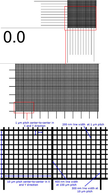
The EM-Tec M-1 has a grid pattern with a pitch of 1 µm and lines at 1, 10 and 100µm. Useful for calibration and image distortion checks in the 100x to 10,000x magnification range.  Alternatively, the samples can be placed directly on the grid pattern for immediate calibration or internal calibration in the image. This is particularly useful for small samples. The lines are etched directly into the ultra flat Si substrate which will give superior signal strength compared to SiO2 etched structures.

Specifications for the EM-Tec M-1 calibration standard with 1 µm pitch grid pattern
Substrate 525µm thick boron doped ultra-flat wafer with <100> orientation
Conductive Excellent; 5-10 Ohm resistivity
Pattern size 3 x 3mm
Pitch/precision 1µm ± 0.025µm, 10µm ± 0.025µm and 100µm ± 0.25µm
Line type /  depth Etched in Si, 300nm ± 30nm deep lines
Line width  200nm ± 10nm for 1µm pitch lines
300nm ± 15nm for 10µm pitch lines
400nm ± 20nm for 100 µm pitch lines
Perpendicularity Better than 0.01°
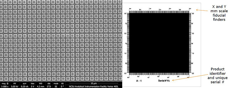
Markers   Edge fiducial markers for grid position finding
Die size 4 x 4mm
Application SEM, FESEM, FIB, Auger, SIMS and reflected light microscopy
Identification Product ID with serial number etched
Mounting Unmounted, mounting optionally available
Supplied  Supplied in a Gel-Pak box
Certification Wafer level certificate of traceability to NIST


EM-Tec M-10 with 10µm pitch grid pattern for 100x to 1000x magnification range


                 EM-Tec M-10 with 10µm pitch grid pattern for 100x to 1000x magnification range
Details EM-Tec M-10 with 10µm pitch grid pattern
for 100x to 1000x magnification range
order info

The EM-Tec M-10 has a grid pattern with a pitch of 10 µm and lines at 10 and 100µm. Useful for calibration and image distortion check in the 100x to 1000x magnification range.  Samples can also be placed directly on the grid pattern for direct calibration or internal calibration in the image. This is practical for small samples. The lines are etched directly into the ultra flat Si substrate which will give superior signal compared to SiO2 etched structures.

Specifications for the EM-Tec M-10 calibration standard with 10 µm pitch grid pattern
Substrate 525µm thick boron doped ultra-flat wafer with <100> orientation
Conductive Excellent; 5-10 Ohm resistivity
Pattern size  3 x 3mm
Pitch/precision 10µm ± 0.025µm and 100µm ± 0.25µm
Line type /  depth Etched in Si, 300nm ± 30nm deep lines
Line width

300nm ± 15nm for 10µm pitch lines\

400nm ± 20nm for 100 µm pitch lines

Perpendicularity Better than 0.01°
Markers Edge fiducial markers for grid position finding
Die size 4 x 4mm
Application SEM, FESEM, FIB, Auger, SIMS and reflected light microscopy
Identification Product ID with serial number etched
Mounting Unmounted, mounting optionally available
Supplied Supplied in a Gel-Pak box
Certification Wafer level certificate of traceability to NIST


Ordering Information

*Prices without VAT, but within the EU, we have to check for valid VAT-ID.
  
EM-Tec M-1 calibration standard with 1µm grid pattern

EM-Tec M-1 with a 1µm pitch grid pattern is useful for calibration or image distortion asessments in the 100x to 10,000x magnification range. Pattern size is 3x3mm with lines directly etched in a conductive ultra-flat silicon substrate. Lines are 300nm deep with a width of 200nm for 1µm lines, 300nm for 10µm lines and 400nm for 100µm lines. Alternatively, small samples can be placed direction on the grid pattern for immediate calibration or integrated calibration in the image. This standard is NIST traceable; example of wafer level certificate of traceability for the Em-Tec M-1 grid pattern calibration standard.
Intended for SEM, FESEM, FIB, Auger, SIMS and reflected light microscopy
 
Product # Unit Price* Add to Quote / Order
31-T34000-U EM-Tec M-1 calibration standard with 1µm grid pattern, unmounted
Qty:

each €95,00
31-T34000-1 EM-Tec M-1 calibration standard with 1µm grid pattern, mounted on standard 12.7mm pin stub
Qty:

each €105,00
31-T34000-2 EM-Tec M-1 calibration standard with 1µm grid pattern, mounted on Zeiss 12.7mm pin stub
Qty:

each €105,00
31-T34000-6 EM-Tec M-1 calibration standard with 1µm grid pattern, mounted on 12.2mm JEOL stub
Qty:

each €122,50
31-T34000-8 EM-Tec M-1 calibration standard with 1µm grid pattern, mounted on 15mm Hitachi stub
Qty:

each €105,00


EM-Tec M-10 calibration standard with 10µm grid pattern

EM-Tec M-10 with a 10µm pitch grid pattern is useful for calibration or image distortion assessments in the 100x to 1000x magnification range. Pattern size is 3x3mm with lines directly etched in a conductive ultra-flat silicon substrate. Lines are 300nm deep with a width of 300nm for 10µm lines and 400nm for 100µm lines. Alternatively, small samples can be placed direction on the grid pattern for immediate calibration or integrated calibration in the image. This standard is NIST traceable; example of wafer level certificate of traceability for the Em-Tec M-10 grid pattern calibration standard.
Intended for SEM, table top SEM, FIB, Auger, SIMS and reflected light microscopy.
 
Product # Unit Price* Add to Quote / Order
31-T35000-U EM-Tec M-10 calibration standard with 10µm grid pattern, unmounted
Qty:

each €95,00
31-T35000-1 EM-Tec M-10 calibration standard with 10µm grid pattern, mounted on standard 12.7mm pin stub
Qty:

each €105,00
31-T35000-2 EM-Tec M-10 calibration standard with 10µm grid pattern, mounted on Zeiss 12.7mm pin stub
Qty:

each €105,00
31-T35000-6 EM-Tec M-10 calibration standard with 10µm grid pattern, mounted on 12.2mm JEOL stub
Qty:

each €122,50
31-T35000-8 EM-Tec M-10 calibration standard with 10µm grid pattern, mounted on 15mm Hitachi stub
Qty:

each €105,00


SEM Supplies

TEM Supplies

Calibration

Sample Preparation

AFM / SPM

  Product Menu with Images
  SEM Sample Stubs
  Carbon Tabs
  Sample Stub Adapters
  SEM Stage Adapters
  SEM Sample Holders
  SEM Preparation Stands
  Filaments / Cathodes
  Silicon Finder Grid
  Gatan 3View Pins
  FEI Volumescope Pins
  SEM Stub Storage Boxes
  Phenom Supplies
  JEOL NeoScope Supplies
  Hitachi TM Series Supplies
  Field & Lab Sampler Kits
  FlowView liquid sample Kit

Instruments

  Acoustic Enclosures
  Compact sputter coaters
  Cressington SEM coaters
  TEM Sample Prep
  Diaphragm Pump
  Rotary vacuum Pump
  Precision diamond saw  
  TEM Grids
  TEM Support Films
  Silicon Nitride Films
  K-Kit Wet Cell Holder
  Graphene Films
  TEM Grid Boxes
  Cryo Grid Boxes
  TEM Sample Staining
  3mm Embedding Tubes
  Filaments/Cathodes
  Eyelash Manipulators

Cryo Supplies

  Cryo Grid Boxes
  Other Cryo Supplies

FIB Supplies

  FIB Lift-out Grids
  FIB Low Profile Stubs
  FIB Grid Holders
  FIB Pre-tilt Holders
  FIB Pre-tilt stubs
  FIB Grid Boxes
  SEM / FIB Magn. Calib.
  SEM Res. Test Spec.
  EDS / WDS Calibration
  TEM Calibration
  AFM / SPM Calibration
  LM Magn. Calibration

Vacuum Supplies

  Vacuum Gauges
  KF/NW Vacuum Parts
  KF/NW Vacuum Hoses
  Vacuum Oil and Grease
  Vacuum Sealant
  Diaphragm Pump
  Rotary vacuum Pump
  Vacuum Sample Storage
  Vacuum Pick-Up Pens

Sample Coating Supplies

  Sputter Targets
  Carbon Rods & Fibers
  Quartz QCM Crystals
  SEM Sample Coating Fluid

Evaporation Supplies

  Thermal Evaporation Sources
  Evaporation Materials
  Supports & Substrates
  SEM Preparation Stands
  Tweezers
  Probes & Picks
  Applicators & Swabs
  Plastic Transfer Pipettes
  Cutting Tools / Scissors
  Conductive Paint/Cement
  Conductive Tapes & Tabs
  Non-Conductive Adhesives
  Sample Storage
  Hand Tools
  Sorting Wire Mesh
  Preparation Surfaces
  Cleaning / Gloves
  Conductive Metal Powders
  Metallographic Sample Prep
  AFM/SPM Discs
  AFM/SPM Disc Pick-up Tool
  AFM/SPM Holders
  AFM/SPM Disc Storage
  Cantilever Tweezers
  AFM/SPM Discs Tweezers
  Nano-Tec Mica Discs
  HOPG Substrates

Light Microscopy

  Correlative Cover Slips
  Glass Microscope Slides
  Glass Cover Slips
  Quartz Microscope Slides
  Quartz Cover Slips
  Black Metal Slides
  Slide Storage Boxes
  LM Calibration
  Plastic Transfer Pipettes
  Optical Lens Tissue
  Glass Petri Dishes
  PTFE Beakers