Nano-Tec gold coated silicon wafers and silicon chips
Introduction
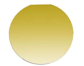
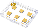
The Nano-Tec gold coated silicon wafers and chips are useful for thin film research, AFM / SPM, nanotechnology and biotechnology applications. The silicon wafers and chips are coated with pure gold over an adhesion layer of Cr. Both Cr and Au are deposited in a dedicated high vacuum deposition system with electron beam evaporation sources. The gold coating is not atomically flat; there are height differences in the nm range. The maximum use temperature is around 175°C; higher temperatures could result in delamination of the gold film. The standard coating thickness is 50nm gold with a 5nm Chromium adhesion layer. Also available are gold coatings with a thickness of 10, 100 and 500 nm.
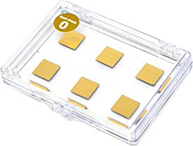
Available in three silicon wafer sizes: Ø2”/51mm, 3”/76mm and Ø4”/100mm and Si chips 10 x 10mm (diced from a 4”/100mm). The Nano-Tec gold coated wafers are individually packed in wafer carrier trays for protection. The Nano-Tec gold coated Si chips are packed in A Gel-Pak box.
Specifications of the Nano-Tec gold coated silicon wafers and chips:
Gold coating |
Coating film Au, 99.999% purity |
50 nm |
10 nm |
100nm |
500nm |
Adhesion film Cr, 99.98% purity |
5 nm |
2 nm |
5 nm |
7.5 nm |
Surface roughness |
Several nm |
Si wafer substrate |
Si substrate Orientation |
<100> |
Si wafer Type |
P (Boron) with one primary flat |
Resistance |
1-30 Ohm/cm |
Si wafer size |
Ø 2”/51 mm |
Ø3”/76mm |
Ø4”/100mm |
10 x 10 mm |
Si wafer thickness |
275µm (+/- 25µm) |
381µm (+/- 25µm) |
525µm (+/- 20µm) |
525µm (+/- 20µm) |
TTV |
=< 20µm |
=< 20µm |
=< 20µm |
n.a. |
Primary Flat |
15.9 +/- 1.65mm |
22.2 +/- 3.17mm |
32.5 +/- 2.5mm |
n.a. |
Ordering information for Nano-Tec gold coated silicon wafers and chips with 50nm gold coating
*Prices without VAT, but within the EU, we have to check for valid VAT-ID.
 |
Nano-Tec gold coated silicon chips, 10 x 10 mm, 525µm thickness, 50nm Au |
| Product # |
Unit |
Price* |
Add to Quote / Order |
| 10-AU8106 |
Nano-Tec gold coated silicon chips, 10 x 10 mm, 525µm thickness, 50nm Au |
|
| pkg/6 |
€225,00
|
| 10-AU8119 |
Nano-Tec gold coated silicon chips, 10 x 10 mm, 525µm thickness, 50nm Au |
|
| pkg/20 |
€485,00
|
|
|
 |
Nano-Tec gold coated silicon wafer, Ø2inch/51mm, 275µm thickness, 50nm Au |
| Product # |
Unit |
Price* |
Add to Quote / Order |
| 10-AU8120-1 |
Nano-Tec gold coated silicon wafer, Ø2”/51mm, 275µm thickness, 50nm Au |
|
| each |
€140,00
|
| 10-AU8120-9 |
Nano-Tec gold coated silicon wafer, Ø2”/51mm, 275µm thickness, 50nm Au |
|
| pkg/9 |
€985,00
|
|
|
|
|
Nano-Tec gold coated silicon wafer, Ø3inch/76mm, 381µm thickness, 50nm Au |
| Product # |
Unit |
Price* |
Add to Quote / Order |
| 10-AU8130-5 |
Nano-Tec gold coated silicon wafer, Ø3inch/76mm, 381um thickness, 50nm Au |
|
| Pkg/5 |
€765,00
|
|
|
|
|
Nano-Tec gold coated silicon wafer, Ø4inch/100mm, 525µm thickness, 50nm Au |
| Product # |
Unit |
Price* |
Add to Quote / Order |
| 10-AU8140-1 |
Nano-Tec gold coated silicon wafer, Ø4inch/100mm, 525um thickness, 50nm Au |
|
| each |
€375,00
|
| 10-AU8140-3 |
Nano-Tec gold coated silicon wafer, Ø4inch/100mm, 525um thickness, 50nm Au |
|
| Pkg/3 |
€980,00
|
|
|
Ordering information for Nano-Tec gold coated wafers with 10nm gold coating
*Prices without VAT, but within the EU, we have to check for valid VAT-ID.
|
|
Nano-Tec gold coated silicon wafer, Ø2inch/51mm, 275µm thickness, 10nm Au |
| Product # |
Unit |
Price* |
Add to Quote / Order |
| 10-AU8126-9 |
Nano-Tec gold coated silicon wafer, Ø2”/51mm, 275µm thickness, 10nm Au |
|
| Pkg/9 |
€855,00
|
|
|
|
|
Nano-Tec gold coated silicon wafer, Ø3inch/76mm, 381µm thickness, 10nm Au |
| Product # |
Unit |
Price* |
Add to Quote / Order |
| 10-AU8131-5 |
Nano-Tec gold coated silicon wafer, Ø3inch/76mm, 381um thickness, 10nm Au |
|
| Pkg/5 |
€855,00
|
|
|
|
|
Nano-Tec gold coated silicon wafer, Ø4inch/100mm, 525µm thickness, 10nm Au |
| Product # |
Unit |
Price* |
Add to Quote / Order |
| 10-AU8141-3 |
Nano-Tec gold coated silicon wafer, Ø4inch/100mm, 525um thickness, 10nm Au |
|
| Pkg/3 |
€855,00
|
|
|
Ordering information for Nano-Tec gold coated silicon wafers and chips with 100nm gold coating
*Prices without VAT, but within the EU, we have to check for valid VAT-ID.
|
|
Nano-Tec gold coated silicon chips, 10 x 10 mm, 525µm thickness, 100nm Au |
| Product # |
Unit |
Price* |
Add to Quote / Order |
| 10-AU8121 |
Nano-Tec gold coated silicon chips, 10 x 10 mm, 525µm thickness, 100nm Au |
|
| pkg/20 |
€545,00
|
|
|
|
|
Nano-Tec gold coated silicon wafer, Ø2inch/51mm, 275µm thickness, 100nm Au |
| Product # |
Unit |
Price* |
Add to Quote / Order |
| 10-AU8127-9 |
Nano-Tec gold coated silicon wafer, Ø2”/51mm, 275µm thickness, 100nm Au |
|
| Pkg/9 |
€1215,00
|
|
|
|
|
Nano-Tec gold coated silicon wafer, Ø3inch/76mm, 381µm thickness, 100nm Au |
| Product # |
Unit |
Price* |
Add to Quote / Order |
| 10-AU8132-5 |
Nano-Tec gold coated silicon wafer, Ø3inch/76mm, 381um thickness, 100nm Au |
|
| Pkg/5 |
€1215,00
|
|
|
|
|
Nano-Tec gold coated silicon wafer, Ø4inch/100mm, 525µm thickness, 100nm Au |
| Product # |
Unit |
Price* |
Add to Quote / Order |
| 10-AU8142-1 |
Nano-Tec gold coated silicon wafer, Ø4inch/100mm, 525um thickness, 100nm Au |
|
| Pkg/1 |
€465,00
|
| 10-AU8142-3 |
Nano-Tec gold coated silicon wafer, Ø4inch/100mm, 525um thickness, 100nm Au |
|
| Pkg/3 |
€1215,00
|
|
|
Ordering information for Nano-Tec gold coated wafers with 500nm gold coating
*Prices without VAT, but within the EU, we have to check for valid VAT-ID.
|
|
Nano-Tec gold coated silicon wafer, Ø2inch/51mm, 275µm thickness, 500nm Au |
| Product # |
Unit |
Price* |
Add to Quote / Order |
| 10-AU8128-9 |
Nano-Tec gold coated silicon wafer, Ø2”/51mm, 275µm thickness, 500nm Au |
|
| Pkg/9 |
€2915,00
|
|
|
|
|
Nano-Tec gold coated silicon wafer, Ø3inch/76mm, 381µm thickness, 500nm Au |
| Product # |
Unit |
Price* |
Add to Quote / Order |
| 10-AU8133-5 |
Nano-Tec gold coated silicon wafer, Ø3inch/76mm, 381um thickness, 500nm Au |
|
| Pkg/5 |
€2915,00
|
|
|
|
|
Nano-Tec gold coated silicon wafer, Ø4inch/100mm, 525µm thickness, 500nm Au |
| Product # |
Unit |
Price* |
Add to Quote / Order |
| 10-AU8143-3 |
Nano-Tec gold coated silicon wafer, Ø4inch/100mm, 525um thickness, 500nm Au |
|
| Pkg/3 |
€2915,00
|
|
|